Datasheet4U Logo Datasheet4U.com

NB3L83948C - 2.5V / 3.3V Differential and LVTTL/LVCMOS 2:1 MUX to 1:12 LVCMOS

Datasheet Summary

Description

The NB3L83948C is a pure 2.5 V / 3.3 V (VDD = VDDO) or mixed mode 3.3 V Core (VDD) / 2.5 V Output (VDDO) clock distribution buffer with the capability to select either a differential LVPECL / LVDS / LVHSTL / SSTL / HCSL or single ended LVCMOS / LVTTL compatible input clock, such as a Primary or a Te

Features

  • 2.5 V / 3.3V (VDD = VDDO) or 3.3 V VDD / 2.5 V VDDO Operation: 2.5 $5%, 2.375 to 2.625 V 3.3 $5%; 3.135 to 3.465 V.
  • 350 MHz Clock Support.
  • Accepts LVPECL, LVDS, LVHSTL, SSTL, HCSL, or LVCMOS Clock Inputs.
  • LVCMOS Compatible Control Inputs.
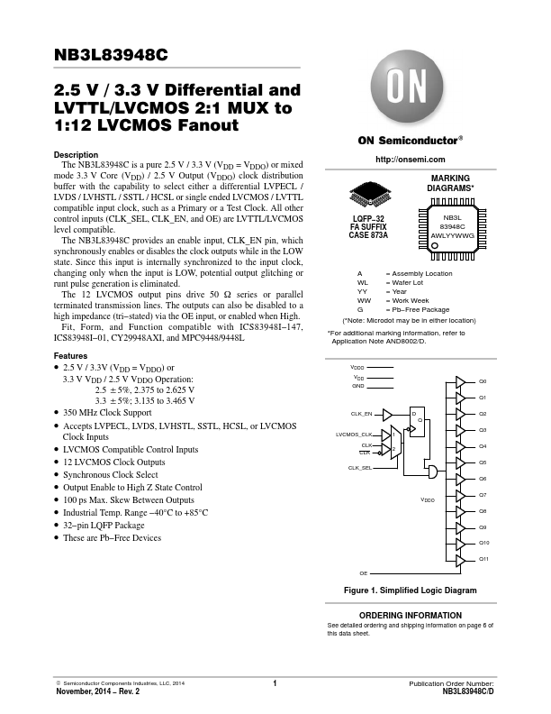
  • 12 LVCMOS Clock Outputs.
  • Synchronous Clock Select.
  • Output Enable to High Z State Control.
  • 100 ps Max. Skew Between Outputs.
  • Industrial Temp. Range.
  • 40°C to +85°C.

📥 Download Datasheet

Datasheet preview – NB3L83948C

Datasheet Details

Part number NB3L83948C
Manufacturer ON Semiconductor
File Size 79.28 KB
Description 2.5V / 3.3V Differential and LVTTL/LVCMOS 2:1 MUX to 1:12 LVCMOS
Datasheet download datasheet NB3L83948C Datasheet
Additional preview pages of the NB3L83948C datasheet.
Other Datasheets by ON Semiconductor

Full PDF Text Transcription

Click to expand full text
NB3L83948C 2.5 V / 3.3 V Differential and LVTTL/LVCMOS 2:1 MUX to 1:12 LVCMOS Fanout Description The NB3L83948C is a pure 2.5 V / 3.3 V (VDD = VDDO) or mixed mode 3.3 V Core (VDD) / 2.5 V Output (VDDO) clock distribution buffer with the capability to select either a differential LVPECL / LVDS / LVHSTL / SSTL / HCSL or single ended LVCMOS / LVTTL compatible input clock, such as a Primary or a Test Clock. All other control inputs (CLK_SEL, CLK_EN, and OE) are LVTTL/LVCMOS level compatible. The NB3L83948C provides an enable input, CLK_EN pin, which synchronously enables or disables the clock outputs while in the LOW state. Since this input is internally synchronized to the input clock, changing only when the input is LOW, potential output glitching or runt pulse generation is eliminated.
Published: |